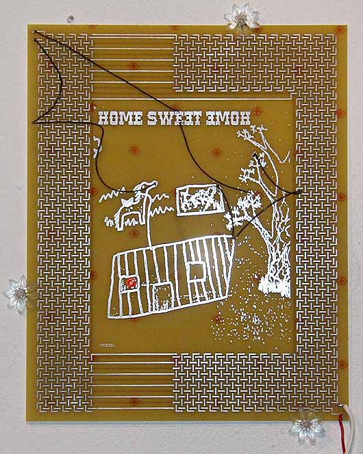
From Paul Slocum:I made a couple of new things for the show, these circuit board pieces. I found a way to translate bitmap images into the circuit design program I was using, and converted actual and recreated images that I had made in elementary and jr. high school. The drawings are rendered in tin-plated copper on standard circuit board material. And the drawings are integrated with very simple circuits that illuminate LEDs and a neon lamp. 
detail of a 12 layer PCB with fine pitch BGAs

detail of the detail

ball pitch is 1 mm
Very pretty. All it needs is a horse tied to a house with a big rope.
Many months ago when I first looked closely at the ball grid array in our PCB artwork, I thought of your molecules. We're starting a new board design, but I don't think we'll incorporate any critters.
I assume (hope) that's something that is read by breaking it down into individual layers.
You're seeing a transparent view. Each distinct layer of copper or silkscreen has its own color. All eight signal layers plus a bit of silkscreen are visible in the small detail. Some of the other colors in the larger detail represent connections to addition layers (power planes). These drawings can be read more easily by selectively turning layers on and off. But usually, following a trace requires turning on multiple layers.
Those lines are about 1/10th of a millimeter. On the real thing, rework (soldering jumper wires, etc.) requires a microscope, and a very steady hand. Back in my day, chips had big old legs that had a pitch of 1/10th of an inch.
So to me, the Paul's work is nostalgic on two levels.
Here's a flash from the past, I came across today. It seems antediluvian, but was produced in my lifetime (barely).
By the way, not all, but some of the detail work on the PCB is hand crafted, still. Little cleanups, straightening jogs, turning 90 degree corners into chamfered turns, etc.
|
From Paul Slocum:
- tom moody 3-21-2005 8:24 pm
detail of a 12 layer PCB with fine pitch BGAs

- mark 4-01-2005 8:04 am
detail of the detail

ball pitch is 1 mm
- mark 4-01-2005 8:20 am
Very pretty. All it needs is a horse tied to a house with a big rope.
- tom moody 4-01-2005 9:36 am
Many months ago when I first looked closely at the ball grid array in our PCB artwork, I thought of your molecules. We're starting a new board design, but I don't think we'll incorporate any critters.
- mark 4-01-2005 10:42 am
I assume (hope) that's something that is read by breaking it down into individual layers.
- tom moody 4-01-2005 10:55 am
You're seeing a transparent view. Each distinct layer of copper or silkscreen has its own color. All eight signal layers plus a bit of silkscreen are visible in the small detail. Some of the other colors in the larger detail represent connections to addition layers (power planes). These drawings can be read more easily by selectively turning layers on and off. But usually, following a trace requires turning on multiple layers.
Those lines are about 1/10th of a millimeter. On the real thing, rework (soldering jumper wires, etc.) requires a microscope, and a very steady hand. Back in my day, chips had big old legs that had a pitch of 1/10th of an inch.
So to me, the Paul's work is nostalgic on two levels.
Here's a flash from the past, I came across today. It seems antediluvian, but was produced in my lifetime (barely).
By the way, not all, but some of the detail work on the PCB is hand crafted, still. Little cleanups, straightening jogs, turning 90 degree corners into chamfered turns, etc.
- mark 4-01-2005 12:00 pm